Maxima mathematical system. Maximum differential Differential amplifiers as comparators
A differential amplifier is a well-known circuit used to amplify the voltage difference of two input signals. Ideally, the output signal does not depend on the level of each of the input signals, but is determined only by their difference. When the signal levels at both inputs change simultaneously, then such a change in the input signal is called common-mode. The differential or difference input signal is also called normal or useful. A good differential amplifier has a high common mode rejection ratio(CMRR), which is the ratio of the wanted output signal to the common-mode output signal, assuming that the wanted and common-mode input signals have the same amplitude. CMRR is usually measured in decibels. The range of variation of the common-mode input signal specifies permissible levels voltage relative to which the input signal should change.
Differential amplifiers are used in cases where weak signals can be lost in the background noise. Examples of such signals are digital signals transmitted over long cables (a cable usually consists of two twisted wires), sound signals(in radio engineering, the concept of “balanced” impedance is usually associated with a differential impedance of 600 Ohms), radio frequency signals (a two-core cable is differential), electrocardiogram voltages, signals for reading information from magnetic memory, and many others. A differential amplifier at the receiving end restores the original signal if the common mode interference is not very large. Differential stages are widely used in the construction of operational amplifiers, which we discuss below. They play an important role in amplifier design direct current(which amplify frequencies up to DC, i.e. do not use capacitors for interstage coupling): their symmetrical circuit is inherently designed to compensate for temperature drift.
In Fig. Figure 2.67 shows the basic circuit of a differential amplifier. The output voltage is measured at one of the collectors relative to ground potential; such an amplifier is called circuit with single-pole output or difference amplifier and it is the most widespread. This amplifier can be thought of as a device that amplifies a differential signal and converts it into a single-ended signal that can be operated regular circuits(voltage repeaters, current sources, etc.). If a differential signal is needed, then it is removed between the collectors.
Rice. 2.67. Classic transistor differential amplifier.
What is the gain of this circuit? It is not difficult to calculate: let’s say a differential signal is applied to the input, and the voltage at input 1 increases by the amount uin (voltage change for a small signal relative to the input).
As long as both transistors are in active mode, the potential of point A is fixed. The gain can be determined as in the case of an amplifier with one transistor, if you notice that the input signal is applied twice to the base-emitter junction of any transistor: K diff = R k /2(r e + R e). The resistance of the resistor R e is usually small (100 Ohms or less), and sometimes this resistor is absent altogether. The differential voltage is usually amplified several hundred times.
In order to determine the common-mode signal gain, the same I/O signals must be applied to both inputs of the amplifier. If you carefully consider this case (and remember that both emitter currents flow through resistor R 1), you will get K sinf = - R k / (2R 1 + R e). We neglect resistance r e, since resistor R 1 is usually chosen to be large - its resistance is at least several thousand ohms. In fact, the resistance R e can also be neglected. CMOS is approximately equal to R 1 (r e + R e). A typical example The differential amplifier is the circuit shown in Fig. 2.68. Let's look at how it works.

Rice. 2.68. Calculation of differential amplifier characteristics.
K diff = U out /(U 1 - U 2) = R to /2(R e + r e):
K diff = R k /(2R 1 + R e + r e);
KOSS ≈ R 1 /(R e + r e).
The resistance of the resistor R k is chosen as follows. so that the quiescent collector current can be taken equal to 100 μA. As usual, to obtain maximum dynamic range, the collector potential is set to 0.5 U kk. Transistor T 1 does not have a collector resistor, since its output signal is removed from the collector of another transistor. The resistance of resistor R 1 is chosen such that the total current is 200 μA and is equally distributed between the transistors when the input (differential) signal equal to zero. According to the formulas just derived, the differential signal gain is 30, and the common mode gain is 0.5. If we exclude 1.0 kOhm resistors from the circuit, then the gain of the differential signal will become equal to 150, but at the same time the input (differential) resistance will decrease from 250 to 50 kOhm (if it is necessary for the value of this resistance to be of the order of megaohms, then transistors can be used in the input stage Darlington).
Let us recall that in an asymmetrical amplifier with a grounded emitter with an output quiescent voltage of 0.5 U kk, the maximum gain is 20 U kk, where U kk is expressed in volts. In a differential amplifier, the maximum differential gain (at R e = 0) is half as much, i.e. numerically equal to twenty times the voltage drop across the collector resistor with a similar choice of operating point. The corresponding maximum CMRR (provided that R e = 0) is also numerically 20 times greater than the voltage drop across R 1 .
Exercise 2.13. Make sure the given ratios are correct. Design a differential amplifier to suit your own requirements.
A differential amplifier can be figuratively called a “long-tailed pair”, since if the length of the resistor is symbol is proportional to the value of its resistance, the circuit can be depicted as shown in Fig. 2.69. The “long tail” determines the common-mode signal rejection, and the small inter-emitter coupling resistances (including the emitters’ own resistances) determine the differential signal amplification.

Biasing using a current source. The common-mode gain in a differential amplifier can be significantly reduced if resistor R 1 is replaced by a current source. In this case, the effective value of resistance R 1 will become very large, and the common-mode signal gain will be weakened almost to zero. Let's imagine that there is a common-mode signal at the input; The current source in the emitter circuit maintains the total emitter current constant, and it (due to the symmetry of the circuit) is evenly distributed between the two collector circuits. Therefore, the output signal of the circuit does not change. An example of such a scheme is shown in Fig. 2.70. For this circuit, which uses a monolithic transistor pair of type LM394 (transistors T 1 and T 2) and a current source of type 2N5963, the CMRR value is determined by the ratio of 100,000:1 (100 dB). The range of the input common-mode signal is limited to -12 and + 7 V: the lower limit is determined by the operating range of the current source in the emitter circuit, and the upper limit is determined by the quiescent collector voltage.

Rice. 2.70. Increasing the CMRR of a differential amplifier using a current source.
Do not forget that this amplifier, like all transistor amplifiers, must have DC mixing circuits. If, for example, a capacitor is used at the input for interstage coupling, then grounded base resistors must be included. Another caveat applies especially to differential amplifiers without emitter resistors: bipolar transistors can withstand no more than 6 V of reverse bias at the base-emitter junction. Then breakdown occurs; This means that if a higher differential input voltage is applied to the input, the input stage will be destroyed (provided that there are no emitter resistors). The emitter resistor limits the breakdown current and prevents destruction of the circuit, but the characteristics of the transistors can degrade in this case (coefficient h 21e, noise, etc.). In either case, the input impedance drops significantly if reverse conduction occurs.
Applications of differential circuits in DC amplifiers with single-pole output. A differential amplifier can work perfectly as a DC amplifier even with single-ended (single-ended) input signals. To do this, you need to ground one of its inputs and send a signal to the other (Fig. 2.71). Is it possible to eliminate the "unused" transistor from the circuit? No. The differential circuit provides compensation for temperature drift, and, even when one input is grounded, the transistor performs some functions: when the temperature changes, the voltage U be changes by the same amount, while no changes occur at the output and the balancing of the circuit is not disrupted. This means that the change in voltage U be is not amplified by the coefficient K diff (its amplification is determined by the coefficient K sinf, which can be reduced to almost zero). In addition, mutual compensation of voltages U be leads to the fact that at the input there is no need to take into account a voltage drop of 0.6 V. The quality of such a DC amplifier deteriorates only due to inconsistency of voltages U be or their temperature coefficients. The industry produces transistor pairs and integrated differential amplifiers with very high degree coordination (for example, for a standard consistent monolithic n-p-n pairs- for transistors of the MAT-01 type, the voltage drift U be is determined by the value of 0.15 μV/°C or 0.2 μV per month).

Rice. 2.71. The differential amplifier can operate as a precision DC amplifier with single-pole output.
In the previous circuit, you can ground any of the inputs. Depending on which input is grounded, the amplifier will or will not invert the signal. (However, due to the presence of the Miller effect, which will be discussed in Section 2.19, the circuit shown here is preferable for the high frequency range). The presented circuit is non-inverting, which means that the inverting input is grounded. The terminology associated with differential amplifiers also applies to operational amplifiers, which are the same high-gain differential amplifiers.
Using a current mirror as an active load. Sometimes it is desirable for a single stage differential amplifier, like a simple grounded emitter amplifier, to have high gain. Beautiful solution gives the use of a current mirror as an active load of an amplifier (Fig. 2.72). Transistors T 1 and T 2 form a differential pair with a current source in the emitter circuit. Transistors T 3 and T 4, forming a current mirror, act as a collector load. This ensures a high value of collector load resistance, thanks to which the voltage gain reaches 5000 and higher, provided that there is no load at the amplifier output. Such an amplifier is usually used only in circuits covered by a loop feedback, or in comparators (we will look at them in the next section). Remember that the load for such an amplifier must have a high impedance, otherwise the gain will be significantly weakened.

Rice. 2.72. Differential amplifier with current mirror as active load.
Differential amplifiers as phase splitting circuits. On the collectors of a symmetrical differential amplifier, signals appear that are identical in amplitude, but with opposite phases. If we take the output signals from two collectors, we get a phase splitting circuit. Of course, you can use a differential amplifier with differential inputs and outputs. The differential output signal can then be used to drive another differential amplifier stage, thereby increasing the CMRR value of the entire circuit significantly.
Differential amplifiers as comparators. Due to its high gain and stable performance, the differential amplifier is the main integral part comparator- a circuit that compares input signals and evaluates which one is larger. Comparators are used in a wide variety of areas: to turn on lighting and heating, to obtain rectangular signals from triangular ones, to compare the signal level with a threshold value, in class D amplifiers and pulse code modulation, to switch power supplies, etc. The main idea when constructing a comparator is that. that the transistor should turn on or off depending on the levels of the input signals. The linear gain region is not considered - the operation of the circuit is based on the fact that one of the two input transistors is in cutoff mode at any time. A typical signal capture application is discussed in the next section using a temperature control circuit that uses temperature-dependent resistors (thermistors).
Differential Gain and Differential Phase are measures of an amplifier's linear distortion. The differential gain is expressed in two quantities, which represent the two peak amplitudes of the subcarrier relative to the amplitude of the black level subcarrier. The differential gain is calculated from the maximum and minimum amplitude of the steps of a special test signal at the output of the demodulator using the oscillogram of the differentiated signal obtained at the output of the measuring differentiating chain with a time constant of 300 ns. Differential phase is expressed in two degrees, which represent the two peak phases of the subcarrier relative to the phase of the black level subcarrier. The differential phase value is calculated as the difference between the maximum and minimum phases of the superimposed element 1 in the level range from black to white. According to EN 50083, in any television channel, the maximum differential gain (peak to peak) must not be more than 14% and the maximum differential phase must not be more than 12%.
Other parameters include input and output impedance, power consumption and supply voltage, weight and dimensions. Let us give as an example the abbreviated specifications of two amplifiers - the main amplifier VX96 from WISI and the universal amplifier DXE 853 GA from Teleste (Table 10.2). The parameters given in the specification should not be considered standard, since they relate to specific amplifier models. Both amplifiers have a forward channel frequency range of 47 – 862 MHz and are equipped with a return channel amplifier module. The amplifiers are equipped with a local or remote power supply. Remote power is supplied through any signal port or built-in power input and can be transmitted in any direction. The VX96 amplifier is designed to create high-quality backbone sections. It is built on the basis of two hybrid chips. A low-noise Push Pull circuit is installed as the input stage, and a powerful silicon or gallium arsenide Push Pull or Power Double circuit is installed as the output stage. The DXE 853 GA amplifier can be used in trunk and home distribution sections of the cable network and has two outputs, configurable by installing taps. Both amplifiers have interstage adjustable EQ and attenuator, replaceable diplexer filters, and space for an optional EQ and attenuator (cable equivalent).
Maximum differential MDPI-028
Maximum differential DMD-70
Maximum differential DMD-70-S
The automatic bimetallic maximum-differential fire detector MDPI-028 is made in a waterproof design and is intended for use on ships. Structurally, the detector is built on two bimetallic elements, which deform when increased ambient temperature and with their loose ends they act on the contacts. Each bimetallic element is located
Automatic bimetallic maximum differential detector MDPI-028 227 ate.
Thermal maximum-differential MDPI-028, the sensitive element is two bimegallic spirals. Triggers at temperature-type + 70° C (+90° C). Controlled area - from 20 to 30 m2. Temperature environment should be between -40 and -50°C. The relative humidity of the premises should not exceed 98%. Works with ship station fire alarm TOL-10/50-S.
The MDPI-028 detector (maximum differential fire detector) in a waterproof design is intended for use in rooms with an air temperature of -40... + 50° C and relative humidity up to 98%. The notice gel is adapted to work in vibration conditions.
To replace morally and technically outdated fire detectors ATIM, ATP, DTL, DI-1, KI-1, RID-1, IDF-1, IDF-1M, POST-1 and control and reception equipment SKPU-1, SDPU- 1, PPKU-1M, TOL-10/100, RUOP-1, new models of modern fire detectors and control panels with significantly better performance indicators of durability, reliability and efficiency, made on a modern element base, were developed and mastered wide application. These included: radioisotope smoke fire detector RID-6M, photoelectric smoke detector DIP-1, DIP-2 and DIP-3, light fire detector ultraviolet radiation IP329-2 “Amethyst” flame detector, explosion-proof thermal fire detector IP-103, thermal magnetic contact multiple-action fire detector IP105-2/1 (ITM), manual fire detector IPR, maximum-differential detector IP101-2, as well as alarm and control devices PPS-3, PPK-2, RUGTI-1, PPKU-1M-01 and Signal-42. To protect explosion and fire hazardous industries, it was developed and transferred to industrial production new intrinsically safe receiving and control device “Signal-44”, designed for connection to an intrinsically safe fire alarm loop
Maximum-differential thermal fire detector is a thermal fire detector that combines the functions of maximum and differential thermal fire detectors.
5 Heat detector IP 129-1 Analogue maximum-differential heat detector
you. Most common heat detectors According to the principle of action, they are divided into maximum, differential and maximum-differential. The first are triggered when a certain temperature is reached, the second - at a certain rate of temperature increase, the third - from any prevailing temperature change. According to their design, heat detectors are passive, in which, under the influence of temperature, sensing element changes its properties (DTL, IP-104-1 - maximum action, based on the opening of spring contacts connected by lightweight solder: MDPT-028 - maximum differential based on the bimetallic effect, leading to deformation of the plates opening the contacts; IP-105- 2/1 - based on the principle of changing magnetic induction under the influence of heat; DPS-38 - differential based on the use of a thermocouple thermopile).
Heat detectors according to their operating principle are divided into maximum, differential and maximum-differential. The first are triggered when a certain temperature is reached, the second - at a certain rate of temperature increase, and the third - from any significant change in temperature. Low-melting locks, bimetallic plates, tubes filled with easily expanding liquid, thermocouples, etc. are used as sensitive elements. Thermal fire detectors are installed under the ceiling in such a position that the heat flow, flowing around the sensitive element of the detector, heats it. Thermal fire detectors are not highly sensitive, so they usually do not give false alarms if the temperature in the room increases when heating is turned on or technological operations are performed.
Thermal or thermal detectors are divided into maximum, differential and maximum-differential.
Maximum-differential detectors are combined, i.e., they operate simultaneously at a certain rate of temperature rise and when critical air temperatures in the room are reached.
Heat detectors according to their operating principle are divided into maximum, differential and maximum-differential.
Differential thermal detectors are triggered at a certain rate of increase in ambient temperature, which is assumed to be within 5-MO°C per minute. Maximum-differential detectors combine the properties of maximum and differential types of detectors.
Heat detectors according to their operating principle are divided into maximum, differential and maximum-differential.
Thermal automatic fire detectors are divided according to their operating principle into maximum, differential and maximum-differential. Detectors of the maximum operating principle are triggered when a certain temperature value is reached, differential - at a certain rate of increase in the temperature gradient, maximum-differential -
Thermal maximum-differential detectors should not be used in the following cases: the rate of change in ambient air temperature is greater than the temperature gradient of the detector response (workshops, hardening, boiler rooms, etc.); there is damp dust (dust concentration is greater than permissible according to sanitary standards).
Fire detectors smoke 215 smoke optical 217 linear volumetric 221 maximum differential
A differential amplifier is a well-known circuit used to amplify the voltage difference of two input signals. Ideally, the output signal does not depend on the level of each of the input signals, but is determined only by their difference. When the signal levels at both inputs change simultaneously, then such a change in the input signal is called common-mode. The differential or difference input signal is also called normal or useful. A good differential amplifier has a high common mode rejection ratio (CMRR), which is the ratio of the desired output signal to the common mode output signal, provided that the desired and common mode input signals are of the same amplitude. CMRR is usually measured in decibels. The range of variation of the common mode input signal specifies the permissible voltage levels relative to which the input signal must vary.
Differential amplifiers are used in cases where weak signals can be lost in the background noise. Examples of such signals are digital signals transmitted over long cables (a cable usually consists of two twisted wires), audio signals (in radio engineering, the concept of “balanced” impedance is usually associated with a differential impedance of 600 ohms), radio frequency signals (a two-core cable is differential), voltage electrocardiograms, signals for reading information from magnetic memory and many others.
Rice. 2.67. Classic transistor differential amplifier.
A differential amplifier at the receiving end restores the original signal if the common mode interference is not very large. Differential stages are widely used in the construction of operational amplifiers, which we discuss below. They play an important role in the design of DC amplifiers (which amplify frequencies down to DC, i.e., do not use capacitors for interstage coupling): their symmetrical circuit is inherently designed to compensate for temperature drift.
In Fig. Figure 2.67 shows the basic circuit of a differential amplifier. The output voltage is measured at one of the collectors relative to ground potential; Such an amplifier is called a single-pole output circuit or a difference amplifier and is the most widely used. This amplifier can be thought of as a device that amplifies a differential signal and converts it into a single-ended signal that can be handled by conventional circuits (voltage followers, current sources, etc.). If a differential signal is needed, then it is removed between the collectors.
What is the gain of this circuit? It is not difficult to calculate: let's say a differential signal is applied to the input, and the voltage at input 1 increases by an amount (voltage change for a small signal relative to the input).
As long as both transistors are in active mode, the potential of point A is fixed. The gain can be determined as in the case of an amplifier with a single transistor, if you notice that the input signal is applied twice to the base-emitter junction of any transistor: . The resistance of the resistor is usually small (100 ohms or less), and sometimes this resistor is absent altogether. The differential voltage is usually amplified several hundred times.
In order to determine the common-mode gain, the same signals must be applied to both inputs of the amplifier. If you look carefully at this case (and remember that both emitter currents flow through the resistor), you will get . We neglect resistance, since the resistor is usually chosen to be large - its resistance is at least several thousand ohms. In fact, resistance can also be neglected. CMRR is approximately equal to . A typical example of a differential amplifier is the circuit shown in Fig. 2.68. Let's look at how it works.
The resistance of the resistor is chosen so that the quiescent collector current can be taken equal to . As usual, the collector potential is set to 0.5 to obtain maximum dynamic range. The transistor does not have a collector resistor, since its output signal is taken from the collector of another transistor. The resistor value is chosen such that the total current is equal and equally distributed between the transistors when the input (differential) signal is zero.

Rice. 2.68. Calculation of differential amplifier characteristics.

According to the formulas just derived, the differential signal gain is 30, and the common mode gain is 0.5. If we exclude 1.0 kOhm resistors from the circuit, then the gain of the differential signal will become equal to 150, but at the same time the input (differential) resistance will decrease from 250 to 50 kOhm (if it is necessary for the value of this resistance to be of the order of megaohms, then in the input stage you can use Darlington transistors).
Recall that in an unbalanced amplifier with a grounded emitter at an output quiescent voltage of 0.5, the maximum gain is equal to , where is expressed in volts. In a differential amplifier, the maximum differential gain (at half as much, i.e., is numerically equal to twenty times the voltage drop across the collector resistor with a similar choice of operating point. The corresponding maximum CMRR (provided that it is also numerically 20 times the voltage drop across
Exercise 2.13. Make sure the given ratios are correct. Design a differential amplifier according to your own requirements.
A differential amplifier can be figuratively called a “long-tailed pair”, since if the length of the resistor in the symbol is proportional to the value of its resistance, the circuit can be depicted as shown in Fig. 2.69. The “long tail” determines the common-mode signal rejection, and the small inter-emitter coupling resistances (including the emitters’ own resistances) determine the differential signal amplification.

Biasing using a current source.
The common mode gain in a differential amplifier can be significantly reduced by replacing the resistor with a current source. In this case, the effective value of the resistance will become very large, and the common-mode signal gain will be attenuated almost to zero. Let's imagine that there is a common-mode signal at the input; The current source in the emitter circuit maintains the total emitter current constant, and it (due to the symmetry of the circuit) is evenly distributed between the two collector circuits. Therefore, the output signal of the circuit does not change. An example of such a scheme is shown in Fig. 2.70. For this circuit, which uses a monolithic transistor pair of type (transistors and ) and a current source of type , the CMRR value is determined by the ratio dB). The input common mode signal range is limited to -12 and ; the lower limit is determined by the operating range of the current source in the emitter circuit, and the upper limit is determined by the quiescent collector voltage.
Rice. 2.70. Increasing the CMRR of a differential amplifier using a current source.
Remember that this amplifier, like all transistor amplifiers, must have DC bias circuits. If, for example, a capacitor is used at the input for interstage coupling, then grounded base resistors must be included. Another caveat applies especially to differential amplifiers without emitter resistors: bipolar transistors can withstand a reverse bias at the base-emitter junction of no more than 6 V, then breakdown occurs; This means that if a higher differential input voltage is applied to the input, the input stage will be destroyed (provided that there are no emitter resistors). The emitter resistor limits the breakdown current and prevents destruction of the circuit, but the characteristics of the transistors can degrade in this case (coefficient, noise, etc.). In either case, the input impedance drops significantly if reverse conduction occurs.
Applications of differential circuits in DC amplifiers with single-pole output.
A differential amplifier can work perfectly as a DC amplifier even with single-ended (single-ended) input signals. To do this, you need to ground one of its inputs and send a signal to the other (Fig. 2.71). Is it possible to eliminate the "unused" transistor from the circuit? No. The differential circuit compensates for temperature drift, and even when one input is grounded, the transistor performs some functions: as the temperature changes, the voltages change by the same amount, while there is no change in the output and the circuit is not unbalanced. This means that the voltage change is not amplified by the coefficient Kdif (its amplification is determined by the coefficient Xinf, which can be reduced to almost zero). In addition, mutual compensation of voltages results in the fact that voltage drops of 0.6 V do not need to be taken into account at the input. The quality of such a DC amplifier deteriorates only due to voltage mismatches or their temperature coefficients. The industry produces transistor pairs and integrated differential amplifiers with a very high degree of matching (for example, for a standard matched monolithic pair of n-p-n-type transistors, the voltage drift is determined by a value or per month).
Rice. 2.71. The differential amplifier can operate as a precision DC amplifier with single-pole output.
In the previous circuit, you can ground any of the inputs. Depending on which input is grounded, the amplifier will or will not invert the signal. (However, due to the presence of the Miller effect, which will be discussed in Section 2.19, the circuit shown here is preferable for the high frequency range.) The presented circuit is non-inverting, which means that the inverting input is grounded. The terminology associated with differential amplifiers also applies to operational amplifiers, which are the same high-gain differential amplifiers.
Using a current mirror as an active load.
Sometimes it is desirable for a single stage differential amplifier, like a simple grounded emitter amplifier, to have high gain. A beautiful solution is provided by using a current mirror as an active load of an amplifier (Fig. 2.72). Transistors form a differential pair with a current source in the emitter circuit. Transistors forming a current mirror act as a collector load. This ensures a high value of the collector load resistance, thanks to which the voltage gain reaches 5000 and higher, provided that there is no load at the amplifier output. Such an amplifier is used, as a rule, only in circuits covered by a feedback loop, or in comparators (we will consider them in the next section). Remember that the load for such an amplifier must have a high impedance, otherwise the gain will be significantly weakened.
Rice. 2.72. Differential amplifier with current mirror as active load.
Differential amplifiers as phase splitting circuits.
On the collectors of a symmetrical differential amplifier, signals appear that are identical in amplitude, but with opposite phases. If we take the output signals from two collectors, we get a phase splitting circuit. Of course, you can use a differential amplifier with differential inputs and outputs. The differential output signal can then be used to drive another differential amplifier stage, thereby increasing the CMRR value of the entire circuit significantly.Differential amplifiers as comparators.
Due to its high gain and stable characteristics, a differential amplifier is the main component of a comparator - a circuit that compares input signals and evaluates which one is greater. Comparators are used in a wide variety of areas: to turn on lighting and heating, to obtain rectangular signals from triangular ones, to compare the signal level with a threshold value, in class D amplifiers and pulse code modulation, to switch power supplies, etc. The basic idea when building a comparator is that the transistor should turn on or off depending on the levels of the input signals. The linear gain region is not considered - the operation of the circuit is based on the fact that one of the two input transistors is in cutoff mode at any time. A typical signal capture application is discussed in the next section using a temperature control circuit that uses temperature-dependent resistors (thermistors).For noise immunity, complementary transmitted signals must be well balanced and have the same impedance
Differential transmission implies the presence of two complementary signals with equal amplitude and a phase shift of 180°. One of the signals is called positive (direct, non-inverse), the second is called negative (inverse). Differential transmission is widely used in electronic circuits and is essential for increasing data transfer speed. High-speed clock signals on computer motherboards and servers are transmitted over differential lines. Numerous devices such as printers, switches, routers and signal processors use LVDS (Low Voltage Differential Signaling) technology.
Compared to single-wire transmission, implementing differential transmission requires a larger number of transmitters (drivers, transmitters) and receivers (receivers), as well as a doubled number of element pins and conductors. On the other hand, using differential transmission offers several attractive advantages:
Greater temporal accuracy,
- high possible transmission speed,
- less susceptibility to electromagnetic interference,
- less noise associated with crosstalk.
When routing differential conductors, it is important that both differential traces have the same impedance, are the same length, and the distance between their edges is constant.
Using an example, let's look at a few important differential wiring concepts. Figure 1 shows the differential bus motherboard, laid between the pins of an application-specific chip (ASIC) and the connector for connecting a daughter board with memory chips. Direct signal conductor highlighted green, and inverse - red. Each conductor along its length has two vias and a serpentine section.
Rice. 1. Differential pair on motherboard PCB
The differential wiring in this figure is made taking into account several rules:
The terminals of components used to transmit or receive differential signals are located close to each other;
- on each individual layer, segments of tires of the same length are located, and the distance between the tires remains the same on different layers;
- when changing a layer, the gap between the via pads is kept to a minimum (not exceeding the distance between the buses, if feasible);
- the serpentine sections of the two buses are located in the same area so that the positive and negative signals have the same propagation delays along the entire length of the circuit.
Rounding corners and uniform lengths of differential conductors require special care.
In addition to conductors printed circuit board, the integrated circuit package contains buses that connect each pin of the package to a pin of the IC chip. The different lengths of these tires can make adjustments in some cases.
As a numerical example, consider differential buses with the following segment lengths:
for direct signal
Segment length from connector pin to first via = 3022.93 mils (76.78 mm),
Segment length between vias = 747.97 mils (19.0 mm)
Total direct signal length = 3,798.70 mils (96.49 mm);
For inverse signal
Segment length from connector pin to first via = 3025.50 mils (76.78 mm),
Segment length between vias = 817.87 mils (19.0 mm)
Segment length from second via to IC pin = 27.8 mils (0.71 mm)
Total length of direct signal circuit = 3,871.17 mils (98.33 mm).
Thus, the difference in PCB trace lengths is 72.47 mils (1.84 mm).
Some of the resulting difference can be compensated by taking into account the different lengths of the buses inside the IC package. In this case, the difference in the total lengths of the routes becomes within the specified tolerance.
Figure 2 shows that total length buses must be thought out from the point of view of reducing the difference in the lengths of differential conductors.
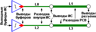
Rice. 2. The sum (L0 + L1) must be equal to the sum (L2 + L3) within the permissible error
Repeating again, it is desirable to keep the distance between the edges of the conductors constant throughout their entire length. A study of the differential pair shows that near the terminals of the bus connector the buses lose parallelism relative to each other. Figure 3 illustrates a wiring diagram that minimizes this drawback while maintaining parallelism on long length(the sharp angle of the inverse signal conductor formed in this case can lead to loss of its integrity with the ensuing consequences - translator's note). This design can be used in cases where differential signals must be highly coupled or when transmitting high-speed signals.
![]()
Rice. 3. Parallel wiring
When the spacing between two traces is relatively large (the coupling between the conductor and the polygon exceeds the coupling between the conductors), the pair becomes loosely coupled. Conversely, when two traces are located close enough to each other (the relationship between them is greater than the connection between the individual conductor and the polygon), then this means that the conductors of the pair are strongly connected. Strong coupling is usually not necessary to achieve the initial benefits of differential structure. However, to achieve good noise immunity, strong coupling is desirable for complementary, well-balanced signals that have symmetrical impedance relative to the reference voltage.
The concept of differential wiring in this case involves coplanar pairs (i.e., located in the same layer), having connections at the edges of the conductors. Differential signals can also be routed in another way, in which the conductors of the direct and inverse signals are located on different (adjacent!!!) layers of the board. However, this method may cause problems with impedance consistency. Figure 4 shows both of these options, as well as some critical dimensions such as width (W), edge spacing (S), conductor thickness (T), and conductor-to-polygon distance (H). These parameters, which establish the cross-sectional geometry of the differential pair, are often used (along with the material properties of the conductors and substrate dielectric) to determine impedance values (for irregular, equilibrium, in-phase, and anti-phase modes) and to calculate the amount of coupling between the conductors of the pair.
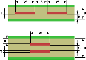
Rice. 4. Geometric dimensions of the differential pair section
Abbas Riazi
DIFFERENTIAL SIGNALS ROUTING REQUIREMENTS
Printed Circuit Design & Manufacture
February-March 2004
We thank the site elart.narod.ru for providing the translation